| CPC H01L 27/124 (2013.01) [G01R 31/28 (2013.01); H01L 21/822 (2013.01); H01L 27/1225 (2013.01)] | 20 Claims |
|
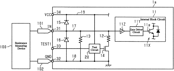
1. A semiconductor device comprising:
a first external terminal to which a first voltage is to be applied;
a second external terminal to which a second voltage is to be applied;
a third external terminal;
first wiring connected to the first external terminal;
second wiring connected to the second external terminal;
a first internal block circuit connected to the first wiring;
a first resistor and a first switching element serially connected between the first wiring and the second wiring;
a second resistor connected between the first wiring and the second wiring; and
a test circuit that is connected to the third external terminal, that turns on and off the first switching element based on a signal from the third external terminal,
wherein a resistance value of the second resistor is larger than a resistance value of the first resistor.
|