US 11,735,596 B2
Semiconductor device comprising oxide semiconductor layer
Shunpei Yamazaki, Setagaya (JP); Jun Koyama, Sagamihara (JP); and Hiroyuki Miyake, Atsugi (JP)
Assigned to Semiconductor Energy Laboratory Co., Ltd., Kanagawa-ken (JP)
Filed by Semiconductor Energy Laboratory Co., Ltd., Atsugi (JP)
Filed on May 24, 2021, as Appl. No. 17/328,171.
Application 17/328,171 is a continuation of application No. 16/780,034, filed on Feb. 3, 2020, granted, now 11,107,840.
Application 16/780,034 is a continuation of application No. 16/391,877, filed on Apr. 23, 2019, granted, now 11,107,838.
Application 16/391,877 is a continuation of application No. 16/277,026, filed on Feb. 15, 2019, granted, now 10,868,046, issued on Dec. 15, 2020.
Application 16/277,026 is a continuation of application No. 14/807,168, filed on Jul. 23, 2015, granted, now 10,249,647, issued on Apr. 2, 2019.
Application 14/807,168 is a continuation of application No. 14/156,845, filed on Jan. 16, 2014, granted, now 9,093,544, issued on Jul. 28, 2015.
Application 14/156,845 is a continuation of application No. 12/938,402, filed on Nov. 3, 2010, granted, now 8,633,480, issued on Jan. 21, 2014.
Claims priority of application No. 2009-255315 (JP), filed on Nov. 6, 2009.
Prior Publication US 2021/0288079 A1, Sep. 16, 2021
Int. Cl. H01L 27/12 (2006.01); H01L 29/04 (2006.01); H01L 29/417 (2006.01); H01L 29/423 (2006.01); H01L 29/10 (2006.01); H01L 29/45 (2006.01); H01L 29/24 (2006.01); G09G 3/20 (2006.01); G11C 19/28 (2006.01); H01L 29/786 (2006.01); H10K 59/121 (2023.01); H01L 29/49 (2006.01)
CPC H01L 27/1229 (2013.01) [G09G 3/20 (2013.01); G11C 19/28 (2013.01); H01L 27/1225 (2013.01); H01L 27/1251 (2013.01); H01L 29/045 (2013.01); H01L 29/1033 (2013.01); H01L 29/24 (2013.01); H01L 29/247 (2013.01); H01L 29/41733 (2013.01); H01L 29/42372 (2013.01); H01L 29/45 (2013.01); H01L 29/7869 (2013.01); H01L 29/78648 (2013.01); H01L 29/78693 (2013.01); G09G 2310/0267 (2013.01); G09G 2310/0275 (2013.01); G09G 2310/0286 (2013.01); H01L 29/4908 (2013.01); H01L 29/78609 (2013.01); H10K 59/1213 (2023.02)] 9 Claims
OG exemplary drawing
 
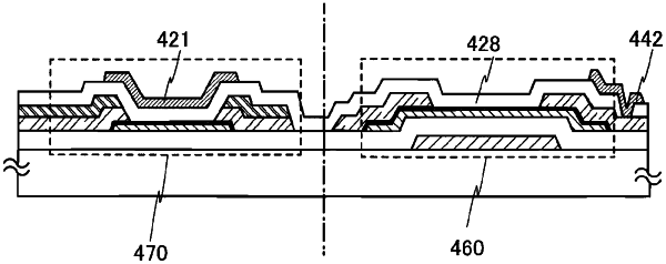
1. A semiconductor device comprising a transistor, the transistor comprising:
an oxide semiconductor layer, in which a channel is formed,
wherein the oxide semiconductor layer comprises In, Sn, Ga, and Zn,
wherein the oxide semiconductor layer comprises a first region comprising crystal grains, in which c-axes are oriented in a direction perpendicular or substantially perpendicular to a surface of the oxide semiconductor layer, in a superficial portion of the oxide semiconductor layer, and
wherein the oxide semiconductor layer comprises a second region comprising an amorphous region which comprises a first microcrystal and a second microcrystal.