| CPC H01L 27/1211 (2013.01) [H01L 29/42384 (2013.01); H01L 29/785 (2013.01)] | 20 Claims |
|
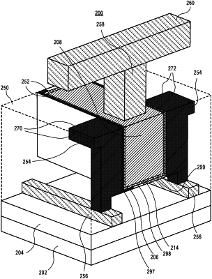
1. An integrated circuit structure, comprising:
an insulator structure above a substrate, the insulator structure having a trench therein, the trench having sidewalls and a bottom;
a channel material layer in the trench in the insulator structure, the channel material layer conformal with the sidewalls and bottom of the trench;
a gate dielectric layer on the channel material layer in the trench, the gate dielectric layer conformal with the channel material layer conformal with the sidewalls and bottom of the trench;
a gate electrode on the gate dielectric layer in the trench, the gate electrode having a first side opposite a second side and having an exposed top surface; a first conductive contact laterally adjacent the first side of the gate electrode, the first conductive contact adjacent a source portion of the channel material layer conformal with the sidewalls of the trench, the source portion of the channel material layer having a first conductivity type; and
a second conductive contact laterally adjacent the second side of the gate electrode, the second conductive contact adjacent a drain portion of the channel material layer conformal with the sidewalls of the trench, the drain portion of the channel material layer having a second conductivity type opposite the first conductivity type.
|