| CPC H01L 27/0251 (2013.01) [G06N 10/00 (2019.01); H01L 29/872 (2013.01); H02H 9/046 (2013.01)] | 20 Claims |
|
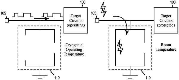
1. A device comprising:
a target circuit that operates at a cryogenic temperature; and
an electrostatic discharge (ESD) protection circuit connected between a terminal of the target circuit and a ground potential, wherein when the ESD protection circuit is configured to, upon receiving a voltage potential at the terminal of the target circuit:
disallow electrical current to flow through the ESD protection circuit from the received voltage potential when the device is at the cryogenic temperature; and
(ii) allow electrical current to flow through the ESD protection circuit from the received voltage potential when the device is at a room temperature.
|