| CPC H01L 25/167 (2013.01) [G02B 6/0006 (2013.01); G02B 6/12004 (2013.01); G02B 6/12007 (2013.01); G02B 2006/12111 (2013.01); G02B 2006/12126 (2013.01)] | 20 Claims |
|
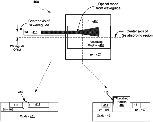
1. An apparatus comprising:
an input waveguide configured to propagate an optical signal along a first dimension; and
a photodiode comprising:
an absorbing region configured to receive the optical signal; and
a semiconductor layer arranged beneath the absorbing region and extending to opposing first and second sides of the absorbing region relative to a second dimension different than the first dimension, wherein the semiconductor layer comprises one or more p-doped regions and one or more n-doped regions arranged such that, along an extent of the semiconductor layer in the first dimension, a location of a P-N junction of the semiconductor layer within the second dimension varies according to a beating pattern of the optical signal.
|