| CPC H01L 25/0657 (2013.01) [H01L 24/08 (2013.01); H01L 24/80 (2013.01); H01L 25/18 (2013.01); H01L 25/50 (2013.01); H01L 2224/08145 (2013.01); H01L 2224/80895 (2013.01); H01L 2224/80896 (2013.01); H01L 2225/0651 (2013.01); H01L 2225/06524 (2013.01); H01L 2225/06555 (2013.01); H01L 2924/1431 (2013.01); H01L 2924/1434 (2013.01)] | 19 Claims |
|
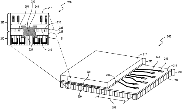
1. A semiconductor die assembly, comprising:
a first semiconductor die including first circuitry; and
a second semiconductor die including second circuitry coupled with the first circuitry, wherein:
the first semiconductor die includes one or more first conductive components and a set of bond pads on a front side of the first semiconductor die, the first conductive components coupled with the first circuitry;
the second semiconductor die includes one or more second conductive components on a front side of the second semiconductor die, the second conductive components coupled with the second circuitry;
the second semiconductor die is arranged over the first semiconductor die such that each of the second conductive components is directly bonded to a corresponding one of the first conductive components; and
a first footprint of the first semiconductor die is larger than a second footprint of the second semiconductor die such that a portion of the front side of the first semiconductor die is exposed, the portion including the set of bond pads.
|