| CPC H01L 24/17 (2013.01) [H01L 23/16 (2013.01); H01L 23/3675 (2013.01); H01L 23/562 (2013.01); H01L 2224/1713 (2013.01); H01L 2224/17051 (2013.01); H01L 2224/17163 (2013.01); H01L 2224/17181 (2013.01); H01L 2224/17519 (2013.01)] | 20 Claims |
|
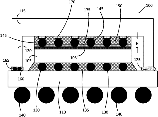
1. A microelectronic package, comprising:
a package substrate;
a die coupled with the package substrate at a first face of the die;
a plurality of solder thermal interface material (STIM) thermal interconnects coupled with the die at a second face of the die in a two-dimensional array pattern, wherein the second face is opposite the first face;
an integrated heat spreader (IHS) coupled with the plurality of STIM thermal interconnects; and
a thermal underfill material positioned between the IHS and the die, wherein the thermal underfill material at least partially surrounds the plurality of STIM thermal interconnects.
|