| CPC H01L 24/14 (2013.01) [H01L 24/11 (2013.01); H01L 24/13 (2013.01); H01L 2224/1146 (2013.01); H01L 2224/11614 (2013.01); H01L 2224/13083 (2013.01); H01L 2224/13111 (2013.01); H01L 2224/13139 (2013.01); H01L 2224/13147 (2013.01); H01L 2224/13155 (2013.01); H01L 2224/14517 (2013.01); H01L 2924/35121 (2013.01)] | 18 Claims |
|
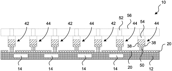
1. A semiconductor device comprising:
a conductive substrate having a first surface and a second surface opposite the first surface;
passivation material covering a portion of the first surface of the conductive substrate;
a first pillar comprising a base layer in contact with the passivation material and a second layer plated to the base layer opposite the passivation material;
a second pillar comprising a base layer in contact with the first surface of the conductive substrate and a second layer in contact with the base layer of the second pillar opposite the first surface of the conductive substrate;
wherein:
the base layer of the first pillar has a first width;
the second layer of the first pillar has a second width greater than the first width;
the base layer of the second pillar has a third width;
the second layer of the second pillar has a fourth width.
|