| CPC H01L 24/05 (2013.01) [H01L 23/3171 (2013.01); H01L 23/3192 (2013.01); H01L 23/528 (2013.01); H01L 27/0658 (2013.01); H01L 27/0664 (2013.01); H01L 27/0676 (2013.01); H01L 28/20 (2013.01); H01L 28/40 (2013.01); H01L 2224/04105 (2013.01); H01L 2224/05558 (2013.01); H01L 2224/05573 (2013.01)] | 17 Claims |
|
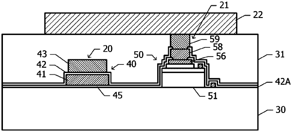
1. A semiconductor device comprising:
a substrate;
a target element to be protected arranged on the substrate;
a protrusion arranged on the substrate;
an insulating film arranged on the substrate and covering the target element and at least a side surface of the protrusion; and
an electrode pad for external connection arranged on the insulating film, the electrode pad at least partially overlapping the target element and the protrusion as seen in plan view,
wherein a maximum distance between an upper surface of the protrusion and the electrode pad in a height direction is shorter than a maximum distance between an upper surface of the target element and the electrode pad in the height direction,
wherein a gap of the insulating film exists between the upper surface of the protrusion and the electrode pad,
wherein the insulating film covers an entire upper surface of the protrusion, and
wherein the substrate is made of a semiconductor, and the protrusion includes an epitaxial semiconductor layer grown from the substrate.
|