| CPC H01L 23/562 (2013.01) [H01L 21/486 (2013.01); H01L 21/4853 (2013.01); H01L 21/4857 (2013.01); H01L 21/565 (2013.01); H01L 21/568 (2013.01); H01L 23/3128 (2013.01); H01L 23/5381 (2013.01); H01L 23/5384 (2013.01); H01L 23/5385 (2013.01); H01L 23/5386 (2013.01); H01L 24/16 (2013.01); H01L 2224/16227 (2013.01); H01L 2924/3511 (2013.01)] | 22 Claims |
|
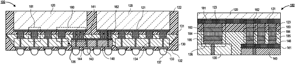
1. An electronic package, comprising:
an interposer, wherein a cavity passes through the interposer;
a nested component in the cavity; and
a die coupled to the interposer by a first interconnect and coupled to the nested component by a second interconnect, wherein the first and second interconnects comprise:
a first bump;
a bump pad over the first bump; and
a second bump over the bump pad.
|