| CPC H01L 23/49838 (2013.01) [H01L 21/4842 (2013.01); H01L 23/49861 (2013.01)] | 3 Claims |
|
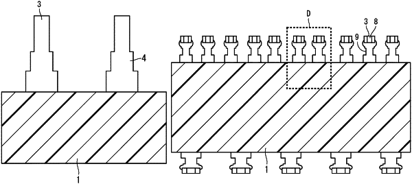
1. A power semiconductor device, comprising:
a package in which a semiconductor element mounted on a lead frame is sealed;
a plurality of terminals exposed from side surfaces of the package and including a first plurality of terminals and a second plurality of terminals;
each of the first plurality of terminals includes:
a tip,
a first contact portion in contact with the package, and
a first terminal bending portion including a first bend, a width of the first bend being larger than a width of the tip and being equal to or smaller than a width of the first contact portion;
each of the second plurality of terminals includes:
a second contact portion in contact with the package, and
a second terminal bending portion including a second bend, a width of the second bend being larger than a width of the second contact portion, wherein
for each of the first plurality of terminals on one of the side surfaces of the package:
concaves are provided on each side of the first terminal bending portion, the concaves being entirely positioned between the first bend and the package, and an entirety of the concaves being located away from the package, and
a width of the first terminal bending portion at the concaves is larger than the width of the tip and is smaller than the width of the first contact portion.
|