| CPC H01L 23/49827 (2013.01) [H01L 23/495 (2013.01); H01L 23/49575 (2013.01); H01L 23/49586 (2013.01); H01L 2224/48137 (2013.01); H01L 2224/48247 (2013.01)] | 20 Claims |

|
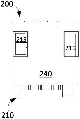
1. An apparatus comprising:
a leadframe including a plurality of leads;
an assembly including a substrate and a plurality of semiconductor die disposed on the substrate, the assembly being coupled to the leadframe;
a molding compound that at least partially encapsulates the leadframe and the assembly; and
an inductor having a first terminal and a second terminal,
the first terminal of the inductor being electrically coupled with a first contact pad of the leadframe, the first contact pad being exposed through a mold cavity defined in the molding compound, at least a portion of the first terminal being recessed in the mold cavity,
the second terminal of the inductor being electrically coupled with a second contact pad of the leadframe, and
the leadframe, the assembly and the inductor being arranged in a stacked configuration.
|