| CPC H01L 23/481 (2013.01) [H01L 21/76232 (2013.01)] | 19 Claims |
|
1. A semiconductor device, comprising:
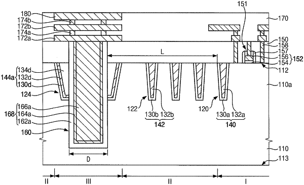
a substrate having a first surface and a second surface opposite to each other, the substrate having a via hole extending in a thickness direction from the first surface;
a circuit pattern in the first surface of the substrate;
a through electrode structure in the via hole;
a first device isolation structure in a first trench extending in one direction in the first surface of the substrate, the first device isolation structure between the via hole and the circuit pattern, the first device isolation structure including a first oxide layer pattern and a first nitride layer pattern sequentially stacked on an inner surface of the first trench, the first nitride layer pattern filling the first trench, and an upper surface of the first nitride layer pattern coplanar with an upper surface of the substrate and an upper surface of the first oxide layer pattern;
a second device isolation structure in a second trench encompassing the through electrode structure, the second device isolation structure including a second oxide layer pattern on an inner surface of the second trench, a second nitride layer pattern on the second oxide layer pattern, and a third oxide layer pattern on the second nitride layer pattern, each of the second oxide layer pattern, the second nitride layer pattern, and the third oxide layer pattern of the second device isolation structure contracting a sidewall of the through electrode structure; and
an insulation interlayer on the first surface of the substrate and covering the circuit pattern.
|