| CPC H01L 23/46 (2013.01) [F28D 15/02 (2013.01); H01L 21/4882 (2013.01); H01L 23/427 (2013.01)] | 14 Claims |
|
1. A microelectronic device package structure, comprising:
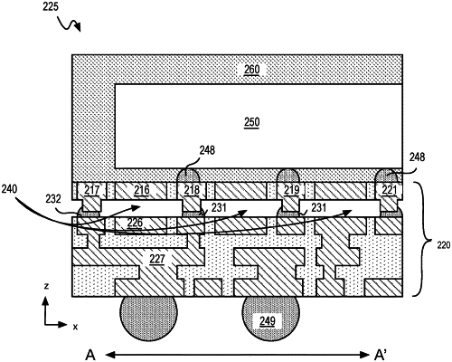
a substrate structure comprising one or more traces adjacent to a mold material, wherein the traces comprise a metal;
an integrated circuit (IC) die physically coupled to the substrate structure, and electrically coupled to at least one of the traces; and
a fluid conduit within the substrate structure, wherein at least a portion of the fluid conduit comprises the metal, and wherein the fluid conduit comprises an inlet to receive a fluid into the substrate structure and an outlet to discharge the fluid from the substrate structure with a length of the fluid conduit therebetween.
|