| CPC H01L 23/367 (2013.01) [H01L 23/3142 (2013.01); H01L 24/32 (2013.01); H01L 24/48 (2013.01); H01L 25/0655 (2013.01); H01L 2224/32225 (2013.01); H01L 2224/48091 (2013.01); H01L 2224/48175 (2013.01)] | 12 Claims |
|
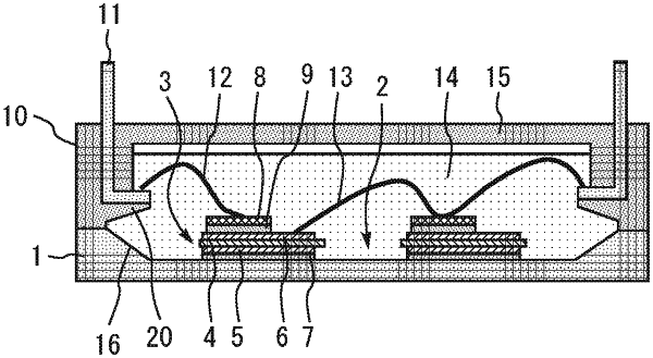
1. A semiconductor module comprising:
a dissipating metal plate including a recess provided on an upper surface;
an insulating substrate provided on a bottom surface of the recess and including a circuit pattern;
a semiconductor device provided on the insulating substrate and connected to the circuit pattern;
a case bonded to a peripheral portion on the upper surface of the dissipating metal plate and surrounding the insulating substrate and the semiconductor device;
a case electrode provided on the case;
a wire connecting the semiconductor device and the case electrode; and
a sealant provided in the case and sealing the insulating substrate, the semiconductor device, and the wire,
wherein a sidewall of the recess has a taper.
|