| CPC H01L 21/76865 (2013.01) [H01L 21/76816 (2013.01); H01L 21/76831 (2013.01); H01L 21/76843 (2013.01); H01L 21/76877 (2013.01)] | 20 Claims |
|
1. A semiconductor device, comprising:
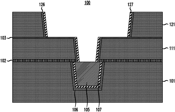
a first interconnect disposed in a first dielectric layer;
a second dielectric layer disposed on the first dielectric layer;
a third dielectric layer disposed on the second dielectric layer;
a second interconnect disposed in a trench in the third dielectric layer, wherein the second interconnect comprises a first portion of a conductive fill layer, wherein a bottom surface of the trench comprises an etch stop layer comprising a conductive material, and wherein the etch stop layer is disposed between the first portion of the conductive fill layer and the second dielectric layer; and
a via disposed in the second dielectric layer, wherein the via comprises a second portion of the conductive fill layer and connects the second interconnect to the first interconnect, and wherein the second portion of the conductive fill layer is disposed on the first interconnect;
wherein the etch stop layer extends along the bottom surface of the trench to inner side surfaces of the trench without extending outside of the trench.
|