| CPC H01L 21/76802 (2013.01) [H01L 21/76877 (2013.01); H01L 23/528 (2013.01); H01L 23/5226 (2013.01)] | 20 Claims |
|
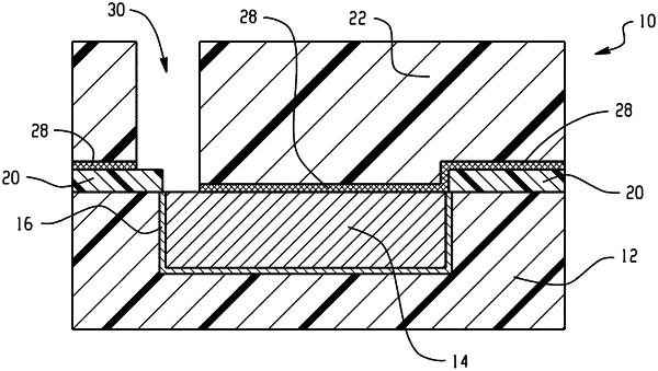
1. A semiconductor device for an integrated circuit, the semiconductor device comprising:
a first interconnect structure disposed above a substrate, the first interconnect structure comprising a metal line formed in a first interlayer dielectric; and
a second interconnect structure overlying the first interconnect structure, the second interconnect structure comprising:
a second cap layer on the first interlayer dielectric;
a second interlayer dielectric thereon; and
at least one self-aligned via in the second interlayer dielectric conductively coupled to at least a portion of the metal line of the first interconnect structure, wherein a misalignment of the at least one self-aligned via results in the at least one self-aligned via landing on both the metal line of the first interconnect structure and the second cap layer, wherein the second cap layer is an insulating material, wherein a portion of the second interlayer dielectric is immediately over the metal line, the portion of the second interlayer dielectric having a bottom surface below a top surface of the second cap layer such that a sidewall face of the second cap layer and a sidewall face of the portion of the second interlayer dielectric are directly opposite one another with the at least one self-aligned via opening in between.
|