| CPC H01L 21/6835 (2013.01) [G11C 8/16 (2013.01); H01L 21/743 (2013.01); H01L 21/76254 (2013.01); H01L 21/76898 (2013.01); H01L 21/8221 (2013.01); H01L 21/823828 (2013.01); H01L 21/84 (2013.01); H01L 23/481 (2013.01); H01L 23/5252 (2013.01); H01L 27/0207 (2013.01); H01L 27/0688 (2013.01); H01L 27/092 (2013.01); H01L 27/10 (2013.01); H01L 27/105 (2013.01); H01L 27/11807 (2013.01); H01L 27/11898 (2013.01); H01L 27/1203 (2013.01); H01L 29/4236 (2013.01); H01L 29/66272 (2013.01); H01L 29/66621 (2013.01); H01L 29/66825 (2013.01); H01L 29/66833 (2013.01); H01L 29/66901 (2013.01); H01L 29/78 (2013.01); H01L 29/7841 (2013.01); H01L 29/7843 (2013.01); H01L 29/7881 (2013.01); H01L 29/792 (2013.01); H10B 10/00 (2023.02); H10B 10/125 (2023.02); H10B 12/053 (2023.02); H10B 12/09 (2023.02); H10B 12/20 (2023.02); H10B 12/50 (2023.02); H10B 20/00 (2023.02); H10B 41/20 (2023.02); H10B 41/40 (2023.02); H10B 41/41 (2023.02); H10B 43/20 (2023.02); H10B 43/40 (2023.02); H01L 23/3677 (2013.01); H01L 24/13 (2013.01); H01L 24/16 (2013.01); H01L 24/45 (2013.01); H01L 24/48 (2013.01); H01L 25/0655 (2013.01); H01L 25/0657 (2013.01); H01L 25/50 (2013.01); H01L 27/1214 (2013.01); H01L 27/1266 (2013.01); H01L 2221/68368 (2013.01); H01L 2223/5442 (2013.01); H01L 2223/54426 (2013.01); H01L 2224/131 (2013.01); H01L 2224/16145 (2013.01); H01L 2224/16146 (2013.01); H01L 2224/16227 (2013.01); H01L 2224/16235 (2013.01); H01L 2224/32145 (2013.01); H01L 2224/32225 (2013.01); H01L 2224/45124 (2013.01); H01L 2224/45147 (2013.01); H01L 2224/48091 (2013.01); H01L 2224/48227 (2013.01); H01L 2224/73204 (2013.01); H01L 2224/73253 (2013.01); H01L 2224/73265 (2013.01); H01L 2224/81005 (2013.01); H01L 2224/83894 (2013.01); H01L 2225/06513 (2013.01); H01L 2225/06541 (2013.01); H01L 2924/00011 (2013.01); H01L 2924/01002 (2013.01); H01L 2924/01004 (2013.01); H01L 2924/01013 (2013.01); H01L 2924/01018 (2013.01); H01L 2924/01019 (2013.01); H01L 2924/01029 (2013.01); H01L 2924/01046 (2013.01); H01L 2924/01066 (2013.01); H01L 2924/01068 (2013.01); H01L 2924/01077 (2013.01); H01L 2924/01078 (2013.01); H01L 2924/01322 (2013.01); H01L 2924/10253 (2013.01); H01L 2924/10329 (2013.01); H01L 2924/12032 (2013.01); H01L 2924/12033 (2013.01); H01L 2924/12036 (2013.01); H01L 2924/12042 (2013.01); H01L 2924/1301 (2013.01); H01L 2924/1305 (2013.01); H01L 2924/13062 (2013.01); H01L 2924/13091 (2013.01); H01L 2924/14 (2013.01); H01L 2924/1461 (2013.01); H01L 2924/1579 (2013.01); H01L 2924/15311 (2013.01); H01L 2924/16152 (2013.01); H01L 2924/181 (2013.01); H01L 2924/19041 (2013.01); H01L 2924/3011 (2013.01); H01L 2924/3025 (2013.01); H01L 2924/30105 (2013.01); H10B 12/05 (2023.02); H10B 20/20 (2023.02)] | 20 Claims |
|
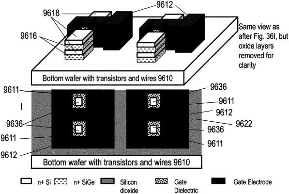
1. A 3D semiconductor device, the device comprising:
a first level comprising a first single crystal layer, said first level comprising first transistors,
wherein each of said first transistors comprises a single crystal channel;
first metal layers interconnecting at least said first transistors;
a second metal layer overlaying said first metal layers; and
a second level comprising a second single crystal layer, said second level comprising second transistors,
wherein said second level overlays said first level,
wherein at least one of said second transistors comprises a gate all around (GAA) transistor structure,
wherein said second level is directly bonded to said first level, and
wherein said bonded comprises direct oxide to oxide bonds.
|