| CPC H01L 21/221 (2013.01) [H01L 21/268 (2013.01); H01L 21/26526 (2013.01); H01L 27/0664 (2013.01); H01L 29/0623 (2013.01); H01L 29/1095 (2013.01); H01L 29/32 (2013.01); H01L 29/404 (2013.01); H01L 29/66348 (2013.01); H01L 29/7397 (2013.01); H01L 29/8613 (2013.01)] | 33 Claims |
|
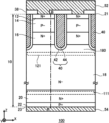
1. A semiconductor device comprising a semiconductor substrate including an upper surface and a lower surface, the semiconductor device further comprising:
a drift region of a first conductivity type provided on the semiconductor substrate;
a base region of a second conductivity type provided between the drift region and the upper surface;
a high concentration region of the first conductivity type or the second conductivity type provided in contact with the lower surface in the semiconductor substrate; and
a buffer region of the first conductivity type provided between the high concentration region and the drift region, the buffer region having one or more donor concentration peaks whose donor concentration is higher than the drift region, wherein
a donor concentration of the drift region is higher than a base doping concentration of the semiconductor substrate, entirely over the drift region in a depth direction connecting the upper surface and the lower surface.
|