| CPC H01L 21/02378 (2013.01) [C23C 16/325 (2013.01); C23C 16/45502 (2013.01); H01L 21/02271 (2013.01); H01L 21/02433 (2013.01)] | 20 Claims |
|
1. A method for manufacturing a silicon carbide epitaxial substrate, the method comprising:
preparing a silicon carbide single-crystal substrate having a first main surface and a second main surface opposite to the first main surface;
placing the silicon carbide single-crystal substrate in a reaction chamber having a substrate placement surface, such that the second main surface faces the substrate placement surface; and
forming a silicon carbide layer on the first main surface by supplying a mixed gas including silane, ammonia, a gas including carbon atoms and hydrogen to the reaction chamber, wherein
the first main surface is a (000-1) plane or a plane inclined by an angle of less than or equal to 8° relative to the (000-1) plane,
the reaction chamber has a cross-sectional area of more than or equal to 132 cm2 and less than or equal to 220 cm2 in a plane perpendicular to a direction of movement of the mixed gas,
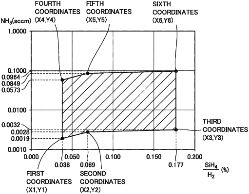
in the forming of the silicon carbide layer, when an X axis indicates a first value representing, in percentage, a value obtained by dividing a flow rate of the silane by a flow rate of the hydrogen, and a Y axis indicates a second value representing a flow rate of the ammonia in sccm, the first value and the second value fall within a hexagonal region surrounded by first coordinates, second coordinates, third coordinates, fourth coordinates, fifth coordinates and sixth coordinates in XY plane coordinates,
the first coordinates are (0.038, 0.0019),
the second coordinates are (0.069, 0.0028),
the third coordinates are (0.177, 0.0032),
the fourth coordinates are (0.038, 0.0573),
the fifth coordinates are (0.069, 0.0849),
the sixth coordinates are (0.177, 0.0964), and
after the forming of the silicon carbide layer, an average value of carrier concentration in the silicon carbide layer is more than or equal to 1×1015 cm−3 and less than or equal to 3×1016 cm−3.
|