| CPC H01G 4/30 (2013.01) [H01G 4/008 (2013.01); H01G 4/012 (2013.01); H01G 4/085 (2013.01); H01G 4/1218 (2013.01)] | 18 Claims |
|
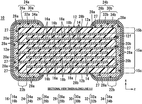
1. A multilayer ceramic electronic component, comprising:
a multilayer body including:
multiple ceramic layers and multiple inner electrode layers that are laminated;
a first main surface and a second main surface opposite to each other in a height direction;
a first side surface and a second side surface opposite to each other in a width direction perpendicular or substantially perpendicular to the height direction; and
a first end surface and a second end surface opposite to each other in a length direction perpendicular or substantially perpendicular to the height direction and the width direction;
a first outer electrode on the first end surface; and
a second outer electrode on the second end surface; wherein
each of the first outer electrode and the second outer electrode includes an underlying electrode layer and a plating layer on the underlying electrode layer;
multiple void portions inside the underlying electrode layer are each filled with a barrier film; and
the barrier film is on a portion of a surface of the underlying electrode layer.
|