US 11,735,269 B2
Secure erase for data corruption
Ting Luo, Santa Clara, CA (US); Kulachet Tanpairoj, Santa Clara, CA (US); Harish Reddy Singidi, Fremont, CA (US); Jianmin Huang, San Carlos, CA (US); Preston Allen Thomson, Boise, ID (US); and Sebastien Andre Jean, Meridian, ID (US)
Assigned to Micron Technology, Inc., Boise, ID (US)
Filed by Micron Technology, Inc., Boise, ID (US)
Filed on Jan. 31, 2022, as Appl. No. 17/589,172.
Application 17/589,172 is a continuation of application No. 17/158,555, filed on Jan. 26, 2021, granted, now 11,238,939.
Application 17/158,555 is a continuation of application No. 16/727,472, filed on Dec. 26, 2019, granted, now 10,950,310.
Application 16/727,472 is a continuation of application No. 15/691,584, filed on Aug. 30, 2017, granted, now 10,522,229.
Prior Publication US 2022/0157386 A1, May 19, 2022
This patent is subject to a terminal disclaimer.
Int. Cl. G11C 8/00 (2006.01); G11C 16/16 (2006.01); G11C 16/04 (2006.01); G11C 16/08 (2006.01); G11C 11/56 (2006.01); G11C 16/34 (2006.01); H10B 41/27 (2023.01); H10B 43/27 (2023.01)
CPC G11C 16/16 (2013.01) [G11C 11/5635 (2013.01); G11C 16/0483 (2013.01); G11C 16/08 (2013.01); G11C 16/3445 (2013.01); G11C 11/5671 (2013.01); G11C 16/3409 (2013.01); H10B 41/27 (2023.02); H10B 43/27 (2023.02)] 20 Claims
OG exemplary drawing
 
1. A memory device comprising:
a memory array of NAND memory cells; and
a memory controller configured to perform operations comprising:
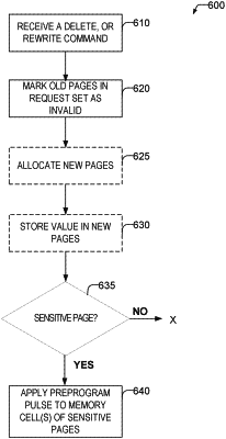
rendering a value stored in a first page of the memory array unreadable by applying a pre-programming pulse to memory cells of the first page without applying an erase pulse until a later garbage collection operation, the pre-programming pulse changing a voltage level of each of the respective memory cells of the first page to a same level.