| CPC G11C 11/5642 (2013.01) [G11C 11/5628 (2013.01); G11C 16/10 (2013.01); G11C 16/26 (2013.01); G11C 16/30 (2013.01)] | 20 Claims |
|
1. A method comprising:
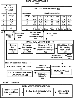
receiving, by a processing device, a request to read data from a block of a memory device coupled with the processing device;
determining, using a data structure which maps block identifiers to voltage distribution parameter values, a voltage distribution parameter value for the block of the memory device;
responsive to determining that a block identifier value for the block is not mapped to any voltage distribution parameter values, determining a corresponding voltage distribution parameter value for the block based on a voltage distribution of one or more memory cells comprised by the block of the memory device;
determining, for the block of the memory device, a set of read levels based on the voltage distribution parameter value, wherein each read level in the set of read levels corresponds to a respective voltage distribution of the memory cells comprised by the block of the memory device; and
reading, using the set of read levels based on the voltage distribution parameter value, data from the block of the memory device.
|