| CPC G09G 3/3266 (2013.01) [G09G 3/325 (2013.01); G09G 3/3291 (2013.01); G09G 2300/0426 (2013.01)] | 18 Claims |
|
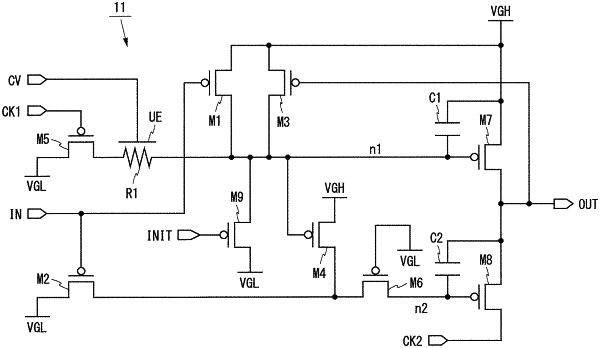
1. A scanning-line driving circuit configured with a plurality of unit circuits cascaded in stages and integrally formed with a display panel, wherein,
the unit circuit includes:
a first transistor that has a first conductive electrode supplied with a first-level voltage and a second conductive electrode connected to a first node;
a resistor connected to the first node at a first terminal;
a second transistor that has a first conductive electrode supplied with a second-level voltage and a second conductive electrode connected to a second terminal of the resistor; and
an output transistor that has a control electrode connected to the first node and a first conductive electrode connected to an output terminal,
the resistor is formed in the same semiconductor layer as semiconductor portions of the first and second transistors, and
the unit circuit further includes an upper electrode formed above the resistor.
|