| CPC G06F 30/392 (2020.01) [G06F 30/31 (2020.01); G06F 30/327 (2020.01); G06F 30/394 (2020.01); G06N 3/045 (2023.01)] | 14 Claims |
|
1. A method for automating a semiconductor design based on artificial intelligence, the method performed by a computing device including at least one processor, the method comprising:
generating a first mask to be placed in a canvas;
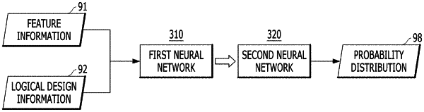
generating a first embedding for a semiconductor element to be placed in the canvas in an area where the first mask is not placed and based on feature information and logical design information of the semiconductor element by using a first neural network; and
generating a probability distribution for placing the semiconductor element based on the first embedding and a second embedding for semiconductor elements already placed in the canvas by using a second neural network,
wherein the first neural network and the second neural network are pre-trained through a reward,
wherein the reward is computed by a weighted sum of a length of a wire connecting the semiconductor elements placed in the canvas, and a congestion of the semiconductor elements placed in the canvas, and
wherein the congestion of the semiconductor elements are maximally evenly distributed.
|