US 11,734,142 B2
Scan synchronous-write-through testing architectures for a memory device
Ming-Hung Chang, Tainan (TW); Atul Katoch, Kanata (CA); Chia-En Huang, Hsinchu County (TW); Ching-Wei Wu, Nantou County (TW); Donald G. Mikan, Jr., Austin, TX (US); Hao-I Yang, Taipei (TW); Kao-Cheng Lin, Taipei (TW); Ming-Chien Tsai, Kaohsiung (TW); Saman M. I. Adham, Kanata (CA); Tsung-Yung Chang, Hsinchu (TW); and Uppu Sharath Chandra, Austin, TX (US)
Assigned to Taiwan Semiconductor Manufacturing Co., Ltd., Hsinchu (TW)
Filed by Taiwan Semiconductor Manufacturing Co., Ltd., Hsinchu (TW)
Filed on Feb. 18, 2022, as Appl. No. 17/651,595.
Application 17/651,595 is a continuation of application No. 16/888,013, filed on May 29, 2020, granted, now 11,256,588.
Application 16/888,013 is a continuation of application No. 15/700,877, filed on Sep. 11, 2017, granted, now 10,705,934, issued on Jul. 7, 2020.
Claims priority of provisional application 62/527,331, filed on Jun. 30, 2017.
Prior Publication US 2022/0171688 A1, Jun. 2, 2022
This patent is subject to a terminal disclaimer.
Int. Cl. G06F 11/263 (2006.01); G06F 1/10 (2006.01); G06F 11/22 (2006.01); G06F 11/267 (2006.01); G11C 29/12 (2006.01); G11C 29/32 (2006.01); G11C 29/48 (2006.01)
CPC G06F 11/263 (2013.01) [G06F 1/10 (2013.01); G06F 11/2273 (2013.01); G06F 11/267 (2013.01); G11C 29/1201 (2013.01); G11C 29/32 (2013.01); G11C 29/48 (2013.01)] 20 Claims
OG exemplary drawing
 
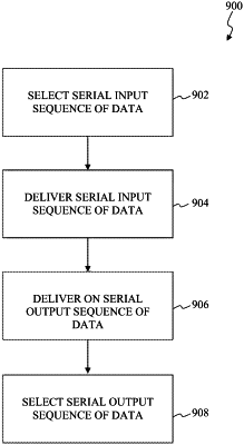
1. A method for operating a memory storage device, the memory storage device including a memory array and circuitry under test, the method comprising:
providing, by first latching circuitry within the memory storage device, an input sequence of data in accordance with a memory clocking signal;
operating on, by the circuitry under test, the input sequence of data to provide a first sequence of output data;
providing, by second latching circuitry within the memory storage device, the input sequence of data as a second sequence of output data in accordance with the memory clocking signal; and
selecting, by multiplexing circuitry within the memory storage device, the first sequence of output data or the second sequence of output data as an output sequence of data.