| CPC G06F 3/0644 (2013.01) [G06F 3/0604 (2013.01); G06F 3/0679 (2013.01)] | 21 Claims |
|
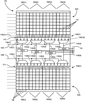
1. A memory array circuit comprising:
a first memory bank; and
a second memory bank;
wherein:
each of the first memory bank and the second memory bank comprises a bank array circuit comprising:
memory bitcell circuits disposed in columns and memory rows;
at least one sub-bank comprising a plurality of memory rows; and
a plurality of column multiplexed (mux) sets, each comprising one or more consecutive columns of the columns, the plurality of column mux sets comprising odd column mux sets alternately disposed with even column mux sets;
a first memory row of a first sub-bank of the at least one sub-bank in the bank array circuit in a first selected bank among the first memory bank and the second memory bank is configured to store:
a first odd data bit of a first data word in the memory bitcell circuit in the one or more consecutive columns of a first odd column mux set of the plurality of odd column mux sets of the first selected bank;
a second odd data bit of the first data word in the memory bitcell circuit in the one or more consecutive columns of a second odd column mux set of the plurality of odd column mux sets of the first selected bank; and
a first even data bit of a second data word in the memory bitcell circuit in the one or more consecutive columns of a first even column mux set of the plurality of even column mux sets of the first selected bank;
a first memory row of a second sub-bank of the at least one sub-bank in the bank array circuit in a second selected bank among the first memory bank and the second memory bank is configured to store a first even data bit of the first data word in the memory bitcell circuit in the one or more consecutive columns of a first even column mux set of the plurality of even column mux sets of the second selected bank; and
the first odd data bit, the first even data bit, and the second odd data bit are consecutive bits of the first data word.
|