| CPC G06F 3/064 (2013.01) [G06F 3/0604 (2013.01); G06F 3/0679 (2013.01)] | 20 Claims |
|
1. A method comprising:
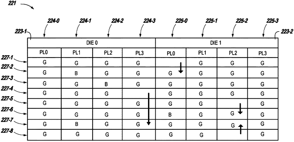
identifying bad blocks in respective planes of a block of non-volatile memory cells of a plurality of blocks of NAND memory cells in a non-volatile memory device;
determining that a plane of the respective planes includes at least one good block in at least one different block of non-volatile memory cells of the plurality of blocks of non-volatile memory cells; and
performing an operation to reallocate the at least one good block in the plane to at least one bad block of the bad blocks in the plane to form a plurality of partial superblocks of non-volatile memory cells each of the partial superblocks having a quantity of bad blocks that satisfies a bad block threshold, wherein the bad block threshold is determined based on a permissible amount of latency that is based on a quantity of permissible bad blocks, in a partial superblock, divided by a quantity of the respective planes of the partial superblock.
|