| CPC G06F 3/0632 (2013.01) [G06F 3/0604 (2013.01); G06F 3/0659 (2013.01); G06F 3/0679 (2013.01); G11C 16/32 (2013.01)] | 16 Claims |
|
1. A memory device comprising:
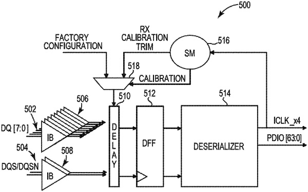
a plurality of input/output (I/O) nodes to receive a plurality of periods of a predefined data pattern;
a circuit to adjust a delay for each I/O node as the predefined data pattern is received;
a latch to latch the data received on each I/O node in response to a data strobe signal;
a memory to store the latched data; and
control logic to:
sweep, via the circuit, the delay for each I/O node to adjust a signal edge for each I/O node as the predefined data pattern is received;
compare the stored latched data to an expected data pattern;
generate a table indicating which stored latched data for each I/O node for each period of the predefined data pattern matches the expected data pattern for each I/O node and which stored latched data for each I/O node for each period of the predefined data pattern does not match the expected data pattern for each I/O node; and
adjust setup and hold time margins for each I/O node by setting, via the circuit, the delay for each I/O node based on the table indicating which stored latched data for each I/O node for each period of the predefined data pattern matches the expected data pattern for each I/O node.
|