| CPC G02B 27/0944 (2013.01) [G02B 5/18 (2013.01); G02B 5/1857 (2013.01); G03F 1/80 (2013.01); G03F 7/0002 (2013.01)] | 20 Claims |
|
1. A method of patterning a substrate, comprising:
forming a hardmask layer on a first side of a substrate, wherein the substrate is formed from a transparent material and is defined by a normal plane along a width of the substrate;
forming, on the hardmask layer, a patterned layer;
etching the patterned layer and the hardmask layer to expose the first side of the substrate;
removing the patterned layer;
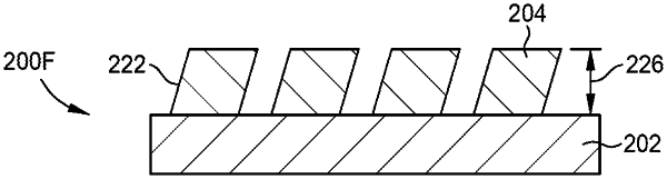
etching the first side of the substrate to form a first plurality of angled mesas in the first side of the substrate, wherein each angled mesa of the first plurality of angled mesas is etched at an angle from 20 degrees to 70 degrees relative to the normal plane;
subsequently, removing the hardmask layer; and
forming a second plurality of angled mesas on a second side of the substrate, the second plurality of angled mesas being at a different angle than the first plurality of angled mesas.
|