| CPC G02B 5/3016 (2013.01) [G02B 1/002 (2013.01); G02B 5/1809 (2013.01); G02B 5/1833 (2013.01); G02B 6/004 (2013.01); G02B 6/0016 (2013.01); G02B 6/0076 (2013.01); G02B 26/103 (2013.01); G02B 27/0081 (2013.01); G02B 27/0172 (2013.01); G02B 27/1006 (2013.01); G02B 27/283 (2013.01); G02B 27/4272 (2013.01); G02F 1/1326 (2013.01); G02B 2027/0112 (2013.01); G02B 2027/0125 (2013.01); G02B 2027/0185 (2013.01); G02F 1/1303 (2013.01)] | 13 Claims |
|
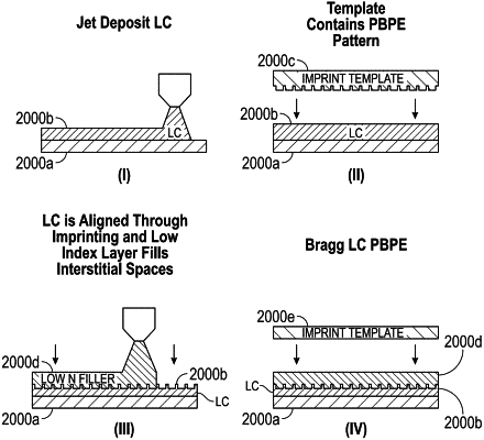
1. A method of manufacturing an optical device including Pancharatnam-Berry Phase Effect (PBPE) structures, the method comprising:
forming an in-coupling optical element comprising the PBPE structures on a waveguide, wherein forming the in-coupling optical element comprises:
disposing a layer of a material that can transmit and/or reflect incident light on the waveguide, wherein the material comprises a liquid crystal; and
imprinting a pattern including PBPE structures on the material.
|