| CPC G01D 5/145 (2013.01) [G01D 11/30 (2013.01)] | 10 Claims |
|
1. A position sensor, comprising:
a detector including
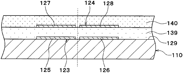
a sensor chip having a surface,
a first detection element disposed at the surface of the sensor chip, and
a second detection element disposed at the surface of sensor chip; and
a signal processor configured to process a signal input from the detector,
wherein the first detection element, which has a first resistance portion and a second resistance portion that are included in a first half-bridge circuit, is configured to output a first detection signal corresponding to a position of a detection target, based on a change in a magnetic field received from the detection target,
wherein the second detection element, which has a third resistance portion and a fourth resistance portion that are included in a second half-bridge circuit, is configured to output a second detection signal corresponding to the position of the detection target, based on the change in the magnetic field received from the detection target,
wherein the third resistance portion, the first resistance portion, the second resistance portion, and the fourth resistance portion are aligned at the surface of the sensor chip in one direction arranged in this order,
wherein the first resistance portion and the second resistance portion are aligned at the surface of the sensor chip to be adjacent to each other in the one direction,
wherein the third resistance portion and the fourth resistance portion are aligned at the surface of the sensor chip to sandwich therebetween the first resistance portion and the second resistance portion in the one direction,
wherein a center of balance of the first detection element is overlapped by a center of balance of the second detection element, and
wherein a wiring pattern of the first half-bridge circuit and a wiring pattern of the second half-bridge circuit coexist at the surface of the sensor chip.
|