| CPC F21V 33/0052 (2013.01) [G01J 1/08 (2013.01); G06F 1/1686 (2013.01); G06F 1/189 (2013.01); G06F 21/32 (2013.01); G06V 40/161 (2022.01); H01S 5/0239 (2021.01); F21Y 2105/16 (2016.08); G01S 7/00 (2013.01); G01S 17/00 (2013.01)] | 20 Claims |
|
1. A light-emitting device comprising:
a wiring substrate;
a base member provided on the wiring substrate;
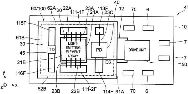
a light-emitting element array that has a first side surface and a second side surface facing each other, that has a third side surface and a fourth side surface facing each other and connecting the first side surface and the second side surface, and that is provided on the base member;
a drive unit that is provided on the wiring substrate at a side of the first side surface and drives the light-emitting element array;
a first circuit element that is provided on the base member at the side of the first side surface;
a second circuit element that is provided on the base member at a side of the second side surface and has a larger occupation area on the base member than the first circuit element; and
wiring members that are provided at a side of the third side surface and at a side of the fourth side surface and extend from an upper surface electrode of the light-emitting element array toward an outer side of the light-emitting element array.
|