| CPC C25D 11/32 (2013.01) [C25F 3/12 (2013.01)] | 19 Claims |
|
1. A method of fabricating a porous silicon carbide structure having a selected morphology, comprising:
providing a silicon carbide structure;
providing an etching solution comprising a reducing agent and an oxidizing agent;
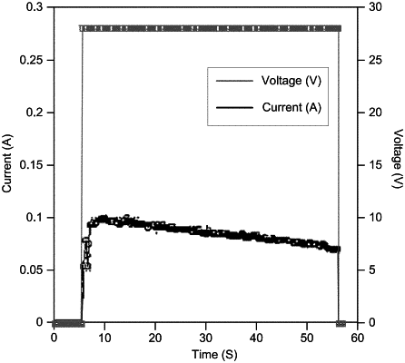
electrochemically etching the silicon carbide structure with the etching solution to produce pores through a region of the silicon carbide structure to form a porous silicon carbide structure, wherein electrochemically etching the silicon carbide structure comprises applying a voltage to a surface of the silicon carbide structure to produce a current through the region of the silicon carbide structure; and
controlling an etch propagation rate of the etching solution through the region of the silicon carbide structure to achieve the selected morphology by changing at least one fabrication parameter including one or more of concentration of reducing agent, voltage, and use of a surfactant, wherein the current decreases at a substantially constant rate during the electrochemical etching step.
|