| CPC C23C 16/458 (2013.01) [C23C 14/50 (2013.01); C23C 16/4586 (2013.01); H01J 37/32715 (2013.01); H01J 37/32724 (2013.01); H01L 21/02274 (2013.01); H01L 21/6831 (2013.01); H05B 3/03 (2013.01)] | 10 Claims |
|
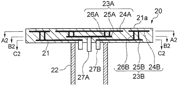
1. A wafer holder comprising:
a ceramic base having a wafer-mounting surface as an upper surface;
a first conductive member embedded in the ceramic base, the first conductive member including
a first circuit portion provided parallel to the wafer-mounting surface,
a first pull-out portion provided parallel to the wafer-mounting surface and spaced from the first circuit portion in a direction opposite to a direction toward the wafer-mounting surface, wherein the first pull-out portion is located in a first layer in a thickness direction of the ceramic base, and
a first plurality of connecting portions configured to electrically connect the first circuit portion and the first pull-out portion to each other;
a second conductive member embedded in the ceramic base, the second conductive member including
at least one second circuit portion provided parallel to the wafer-mounting surface,
at least one second pull-out portion provided parallel to the wafer-mounting surface and spaced from the at least one second circuit portion in the direction opposite to the direction toward the wafer-mounting surface, wherein the at least one second pull-out portion is located in a second layer in the thickness direction of the ceramic base, the second layer being spaced from the first layer in the thickness direction, and
a second plurality of connecting portions configured to electrically connect the at least one second circuit portion and the at least one second pull-out portion to each other;
a cylindrical support configured to support a lower surface of the ceramic base; and
an electrode terminal portion connected to the first pull-out portion, wherein
a portion of the electrode terminal portion protrudes from the lower surface of the ceramic base and is housed in the cylindrical support, and
the first plurality of connecting portions are arranged in a circumferential direction at an outer circumferential portion of the first pull-out portion.
|