| CPC B23K 3/0623 (2013.01) [H01L 21/486 (2013.01); H01L 21/4857 (2013.01); H01L 23/3735 (2013.01); H01L 23/49822 (2013.01); H05K 3/3468 (2013.01); H01L 2924/014 (2013.01); H01L 2924/1517 (2013.01); H01L 2924/15312 (2013.01)] | 30 Claims |

|
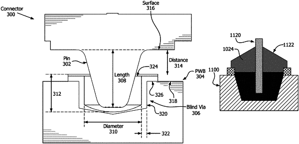
1. A method for providing a soldered interface between a circuit board and a pin, comprising:
applying first solder directly to the pin by
disposing a given amount of first solder on a non-wettable surface of a planar substrate,
inserting the pin in the first solder, and
performing a reflow process to cause the first solder to transfer from the planar substrate to the pin without soldering the pin to the planar substrate;
using a jet paste dispenser to apply second solder into a plated contact cavity formed in the circuit board;
using a stencil screen printer to apply third solder (a) over the plated contact cavity which was at least partially filled with the second solder by the jet paste dispenser and (b) over at least a portion of a pad surrounding the plated contact cavity;
inserting the pin with the first solder applied thereto in the plated contact cavity such that the pin passes through the third solder and extends at least partially through the second solder; and
performing a reflow process to heat the first, second and third solder so as to create a solder joint between the circuit board and the pin.
|