| CPC H01L 24/81 (2013.01) [H01L 24/13 (2013.01); H01L 24/14 (2013.01); H01L 24/16 (2013.01); H01L 2224/13013 (2013.01); H01L 2224/13016 (2013.01); H01L 2224/13144 (2013.01); H01L 2224/13466 (2013.01); H01L 2224/14051 (2013.01); H01L 2224/16057 (2013.01); H01L 2224/80201 (2013.01); H01L 2224/80986 (2013.01); H01L 2224/81053 (2013.01); H01L 2224/81193 (2013.01); H01L 2224/81203 (2013.01); H01L 2224/81379 (2013.01)] | 11 Claims |
|
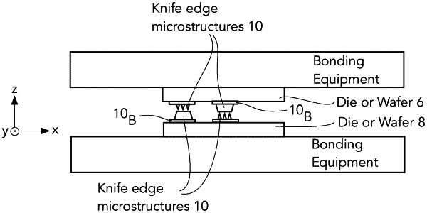
1. An electronic component, die or wafer, comprising:
a first array of microstructures on a major surface of the electronic component, die or wafer that project in a direction essentially normal to the major surface, the microstructures each terminating at a distal end thereof with an elongate edge spaced at a height h from the major surface; and
a second array of structures on the major surface having flat, planar surfaces spaced at a height h′ from the major surface, the height h′ being no more than one half the height h;
wherein the first array of microstructures are formed adjacent to and spaced apart from the second array of microstructures on the major surface of the electronic component;
wherein the first array of microstructures are configured to have a plurality of layers parallel to the major surface with alternating hardnesses,
wherein the first array of microstructures are configured to temporarily bond with a corresponding array of microstructures formed on a second electronic component, die or wafer, before the second array of structures permanently bonding with a corresponding array of structures of the second electronic component, die or wafer.
|