US 12,041,799 B2
Imaging element, stacked-type imaging element, imaging apparatus, and manufacturing method of imaging element
Yasuharu Ujiie, Kanagawa (JP); Ichiro Takemura, Kanagawa (JP); Masaki Orihashi, Kanagawa (JP); and Yohei Hirose, Kanagawa (JP)
Assigned to Sony Group Corporation, Tokyo (JP); and Sony Semiconductor Solutions Corporation, Kanagawa (JP)
Filed by SONY GROUP CORPORATION, Tokyo (JP); and SONY SEMICONDUCTOR SOLUTIONS CORPORATION, Kanagawa (JP)
Filed on Jun. 16, 2022, as Appl. No. 17/842,506.
Application 17/842,506 is a continuation of application No. 16/466,387, granted, now 11,495,762, previously published as PCT/JP2017/037573, filed on Oct. 17, 2017.
Claims priority of application No. 2016-244224 (JP), filed on Dec. 16, 2016.
Prior Publication US 2022/0310951 A1, Sep. 29, 2022
This patent is subject to a terminal disclaimer.
Int. Cl. H01L 27/28 (2006.01); H01L 27/30 (2006.01); H01L 51/42 (2006.01); H01L 51/44 (2006.01); H10K 19/20 (2023.01); H10K 30/30 (2023.01); H10K 30/82 (2023.01); H10K 30/87 (2023.01); H10K 39/32 (2023.01); H10K 85/60 (2023.01); H01L 27/146 (2006.01)
CPC H10K 30/87 (2023.02) [H10K 19/20 (2023.02); H10K 30/30 (2023.02); H10K 30/82 (2023.02); H10K 39/32 (2023.02); H10K 85/636 (2023.02); H01L 27/14647 (2013.01); H10K 85/655 (2023.02); H10K 85/6572 (2023.02)] 12 Claims
OG exemplary drawing
 
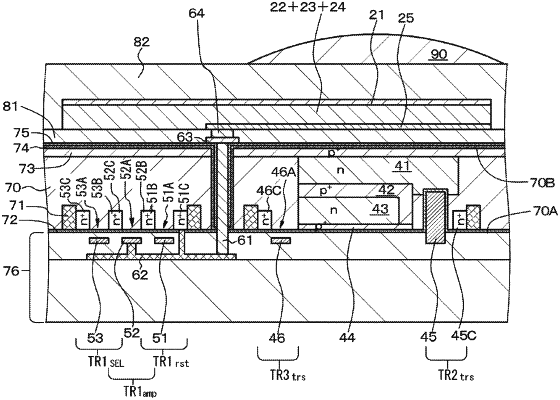
1. A light detecting element comprising:
a first electrode;
a second electrode;
a photoelectric conversion layer disposed between the first electrode and the second electrode; and
a buffer layer disposed between the first electrode and the photoelectric conversion layer,
wherein the photoelectric conversion layer comprises quinacridone derivatives or a thienoacene-based material, and
wherein the buffer layer includes a material having structural formula (4) or structural formula (5):

OG Complex Work Unit Chemistry
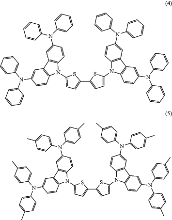
in which thiophene and carbazole are combined.