| CPC H10B 43/35 (2023.02) [G11C 16/0483 (2013.01); H10B 43/10 (2023.02); H10B 43/20 (2023.02)] | 15 Claims |
|
1. A semiconductor storage device comprising:
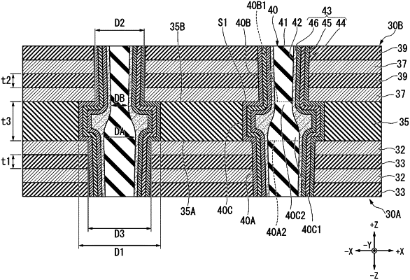
a first stacked body including a plurality of conductive layers and a plurality of insulating layers that are alternately stacked;
a second stacked body being located above the first stacked body and including a plurality of conductive layers and a plurality of insulating layers that are alternately stacked;
an intermediate insulating layer being located between the first stacked body and the second stacked body, the intermediate insulating layer having a thickness in the stacking direction larger than that of one of the plurality of insulating layers of the first stacked body; and
a plurality of columnar bodies provided over the first stacked body and the second stacked body, each columnar body including a core, a charge storage film provided between at least one of the plurality of conductive layers and the core, and a semiconductor body provided between the charge storage film and the core, wherein
each of the plurality of columnar bodies includes (i) a first columnar portion formed in the first stacked body, (ii) an intermediate columnar portion formed in the intermediate insulating layer, and (iii) a second columnar portion formed in the second stacked body, and
wherein a width of the semiconductor body in the intermediate columnar portion in a direction intersecting the stacking direction is (i) relatively thinnest at an upper end of the intermediate columnar portion, and (ii) relatively thickest at a lower end of the intermediate columnar portion.
|