| CPC H01L 33/58 (2013.01) [H01L 21/565 (2013.01); H01L 23/3135 (2013.01); H01L 31/0203 (2013.01); H01L 31/02327 (2013.01); H01L 31/18 (2013.01); H01L 33/005 (2013.01); H01L 33/54 (2013.01); H01L 2933/005 (2013.01); H01L 2933/0058 (2013.01)] | 11 Claims |
|
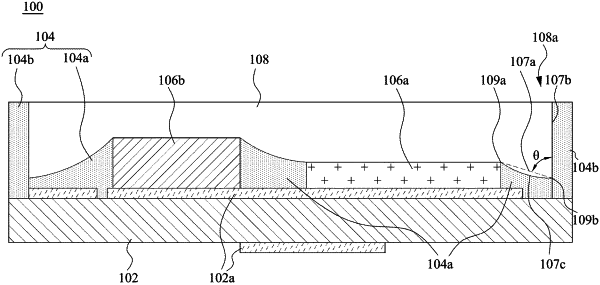
1. A diode package structure comprising:
a substrate having an electrically conductive layer;
a first diode chip and a second diode chip disposed on the substrate and electrically connected to the electrically conductive layer; and
an opaque encapsulating layer having a first cap portion, a second cap portion, and a sidewall portion, wherein the sidewall portion is connected to and surrounds the substrate to jointly form a concave structure, the first cap portion is connected between a sidewall of the first diode chip and the sidewall portion, wherein a first contact vertex of the first cap portion and the sidewall of the first diode chip is higher than a second contact vertex of the first cap portion and the sidewall portion,
wherein the second cap portion is disposed between the first diode chip and the second diode chip, a third contact vertex of the second cap portion and the first diode chip is lower than a fourth contact vertex of the second cap portion and the second diode chip.
|