| CPC H01L 29/41766 (2013.01) [H01L 21/0465 (2013.01); H01L 21/2652 (2013.01); H01L 21/26553 (2013.01); H01L 21/76232 (2013.01); H01L 29/401 (2013.01); H01L 21/266 (2013.01); H01L 29/0847 (2013.01); H01L 29/16 (2013.01); H01L 29/1608 (2013.01); H01L 29/20 (2013.01); H01L 29/2003 (2013.01)] | 8 Claims |
|
1. A semiconductor structure comprising:
a first silicon germanium layer;
a second silicon germanium layer;
a silicon layer between the first and second silicon germanium layers;
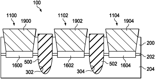
first and second shallow trench isolation structures extending through the first silicon germanium layer, the silicon layer and the second silicon germanium layer;
a first cavity on one side of the first shallow trench isolation structure, a second cavity between the first and second shallow trench isolation structures, and a third cavity on one side of the second shallow trench isolation structure;
first, second, and third active areas below the respective first, second and third cavities, wherein the first, second and third active areas are in contact with the silicon layer; and
first, second and third metal contacts in the respective first, second and third cavities, wherein the first, second and third metal contacts are formed by depositing metal in the first, second and third cavities, respectively, and wherein the first, second and third metal contacts are isolated from the silicon layer by the respective first, second and third active areas.
|