| CPC H01L 29/401 (2013.01) [H01L 21/02329 (2013.01); H01L 21/283 (2013.01); H01L 21/3115 (2013.01); H01L 21/8221 (2013.01); H01L 21/823462 (2013.01); H01L 21/823857 (2013.01); H01L 27/0922 (2013.01); H01L 29/42392 (2013.01); H01L 29/66439 (2013.01)] | 20 Claims |
|
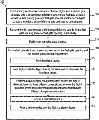
1. A method comprising:
forming a first semiconductor layer stack having a first upper semiconductor layer over a first lower semiconductor layer and a second semiconductor layer stack having a second upper semiconductor layer over a second lower semiconductor layer;
forming high-k dielectric layers over the first upper semiconductor layer, the second upper semiconductor layer, the first lower semiconductor layer, and the second lower semiconductor layer, wherein the high-k dielectric layers have a same composition; and
performing a dipole engineering process to cause the high-k dielectric layers to have different compositions, wherein the dipole engineering process includes a nitrogen-containing thermal drive-in process and, after the dipole engineering process, at least two of the high-k dielectric layers have different dipole dopant concentrations and at least two of the high-k dielectric layers have different nitrogen concentrations.
|