US 12,040,358 B2
Method of manufacturing a super junction structure and super junction structure
Shuai Zhang, Hsinchu (TW); Feng Han, Hsinchu (TW); Jian Wu, Hsinchu (TW); Lian-Jie Li, Hsinchu (TW); and Zhong-Hao Chen, Hsinchu (TW)
Assigned to TAIWAN SEMICONDUCTOR MANUFACTURING COMPANY, LTD., Hsinchu (TW)
Filed by TAIWAN SEMICONDUCTOR MANUFACTURING COMPANY, LTD., Hsinchu (TW)
Filed on Nov. 9, 2021, as Appl. No. 17/454,168.
Application 16/855,253 is a division of application No. 14/586,453, filed on Dec. 30, 2014, abandoned.
Application 17/454,168 is a continuation of application No. 16/855,253, filed on Apr. 22, 2020, granted, now 11,201,211.
Claims priority of application No. 201410614306.6 (CN), filed on Nov. 4, 2014.
Prior Publication US 2022/0069074 A1, Mar. 3, 2022
This patent is subject to a terminal disclaimer.
Int. Cl. H01L 29/06 (2006.01); H01L 21/225 (2006.01); H01L 21/265 (2006.01); H01L 29/417 (2006.01); H01L 29/66 (2006.01); H01L 29/78 (2006.01)
CPC H01L 29/0634 (2013.01) [H01L 29/41741 (2013.01); H01L 29/66734 (2013.01); H01L 29/7809 (2013.01); H01L 29/7813 (2013.01); H01L 21/2253 (2013.01); H01L 21/26506 (2013.01); H01L 21/26513 (2013.01); H01L 29/66727 (2013.01)] 19 Claims
OG exemplary drawing
 
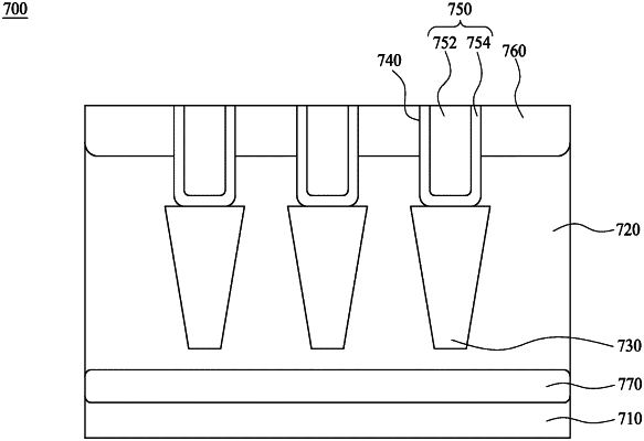
1. A method of manufacturing a super junction structure, the method comprising:
etching a material to define a trench, wherein the trench has a tapered profile;
implanting dopants into borders of the trench to define a doped region surrounding the trench;
depositing an undoped polymer material into the trench; and
driving the dopants from the doped region into the undoped polymer material.