| CPC H01L 25/167 (2013.01) [H01L 23/481 (2013.01); H01L 23/52 (2013.01); H01L 23/535 (2013.01); H01L 27/124 (2013.01); H01L 33/60 (2013.01); H01L 33/62 (2013.01); G09G 3/22 (2013.01); H01L 33/44 (2013.01)] | 20 Claims |
|
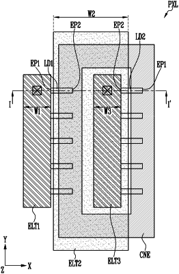
1. A display device comprising:
a substrate;
a passivation layer above a substantial entirety of the substrate;
a first electrode extending in a first direction above the passivation layer, and having a first width in a second direction crossing the first direction in plan view;
a second electrode extending in the first direction entirely below the passivation layer, and having a second width in the second direction in plan view that is greater than the first width;
a first light emitting element on a same layer as the first electrode; and
a contact electrode on the first light emitting element,
wherein one end of the first light emitting element contacts the first electrode, and another end of the first light emitting element contacts the contact electrode.
|