US 12,040,283 B2
Method of fabricating semiconductor structure
Tzu-Sung Huang, Tainan (TW); Cheng-Chieh Hsieh, Tainan (TW); Hsiu-Jen Lin, Hsinchu County (TW); Hui-Jung Tsai, Hsinchu (TW); Hung-Yi Kuo, Taipei (TW); Hao-Yi Tsai, Hsinchu (TW); Ming-Hung Tseng, Miaoli County (TW); Yen-Liang Lin, Taichung (TW); Chun-Ti Lu, Hsinchu (TW); and Chung-Ming Weng, Hsinchu (TW)
Assigned to Taiwan Semiconductor Manufacturing Company, Ltd., Hsinchu (TW)
Filed by Taiwan Semiconductor Manufacturing Company, Ltd., Hsinchu (TW)
Filed on Apr. 19, 2023, as Appl. No. 18/303,543.
Application 17/666,579 is a division of application No. 16/881,002, filed on May 22, 2020, granted, now 11,244,906, issued on Feb. 8, 2022.
Application 18/303,543 is a continuation of application No. 17/666,579, filed on Feb. 8, 2022, granted, now 11,664,325.
Prior Publication US 2023/0275030 A1, Aug. 31, 2023
This patent is subject to a terminal disclaimer.
Int. Cl. H01L 23/48 (2006.01); H01L 21/56 (2006.01); H01L 21/78 (2006.01); H01L 23/00 (2006.01); H01L 23/31 (2006.01); H01L 23/538 (2006.01); H01L 25/00 (2006.01); H01L 25/065 (2023.01)
CPC H01L 23/5389 (2013.01) [H01L 21/56 (2013.01); H01L 21/78 (2013.01); H01L 23/3121 (2013.01); H01L 24/94 (2013.01); H01L 25/0657 (2013.01); H01L 25/50 (2013.01)] 20 Claims
OG exemplary drawing
 
1. A method, comprising:
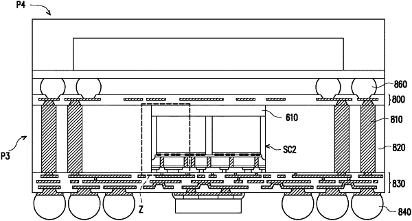
placing first semiconductor dies to a semiconductor wafer comprising second semiconductor dies, the semiconductor wafer comprising a semiconductor substrate and an interconnect structure disposed on the semiconductor substrate;
forming grooves on the semiconductor wafer, the grooves extending through the interconnect structure, and the semiconductor substrate being revealed by the grooves;
forming an insulating encapsulation over the semiconductor wafer to laterally encapsulate the first semiconductor dies and fill the grooves; and
performing a wafer sawing process to saw the insulating encapsulation and the semiconductor wafer along the grooves, wherein a portion of the insulating encapsulation remains on sidewalls of the interconnect structure after performing the wafer sawing process.