| CPC H01L 23/427 (2013.01) [H01L 23/5226 (2013.01); H01L 27/1203 (2013.01)] | 17 Claims |
|
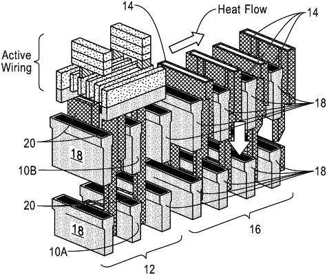
1. A semiconductor structure comprising:
vertically stacked field effect transistors located in an electrically active device area of the semiconductor structure; and
an electrically inactive structure located in an electrically inactive device area of the semiconductor structure that is located adjacent to the electrically active device area of the semiconductor structure, wherein the electrically inactive structure comprises at least one vertical interconnect structure that continuously extends from an uppermost layer of the vertically stacked field effect transistors to a bottommost layer of the vertically stacked field effect transistors.
|