| CPC H01L 21/7682 (2013.01) [H01L 21/76805 (2013.01); H01L 21/76895 (2013.01); H01L 23/53257 (2013.01); H01L 23/5329 (2013.01); H01L 23/535 (2013.01); H10B 41/27 (2023.02); H10B 43/27 (2023.02)] | 14 Claims |
|
1. A microelectronic device, comprising:
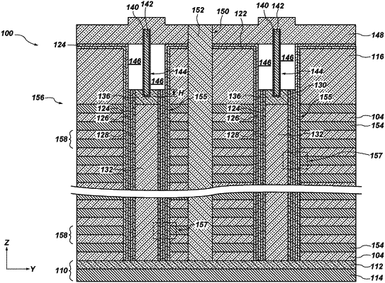
a stack structure comprising a vertically alternating sequence of conductive structures and insulative structures arranged in tiers;
strings of memory cells vertically extending through the stack structure, the strings of memory cells individually comprising a channel material vertically extending through the stack structure;
a conductive contact structure vertically overlying and in electrical communication with the channel material of a string of memory cells of the strings of memory cells;
a void laterally neighboring the conductive contact structure and directly vertically above and contacting, laterally overlapping, and partially defined by an upper surface of the channel material of the string of memory cells, the conductive contact structure separated from a laterally neighboring conductive contact structure by the void, a dielectric material, and an additional void laterally neighboring the laterally neighboring conductive contact structure;
wherein the void comprises an annular cross-sectional shape; and
wherein a dielectric constant of the void is within a range from about 1.0 to about 1.5.
|