US 12,040,182 B2
Plasma doping of gap fill materials
Santanu Sarkar, Boise, ID (US); Jay Steven Brown, Boise, ID (US); Shu Qin, Boise, ID (US); Yongjun Jeff Hu, Boise, ID (US); and Farrell Martin Good, Meridian, ID (US)
Assigned to Micron Technology, Inc., Boise, ID (US)
Filed by Micron Technology, Inc., Boise, ID (US)
Filed on Oct. 21, 2022, as Appl. No. 17/971,376.
Application 17/971,376 is a division of application No. 15/930,875, filed on May 13, 2020, granted, now 11,508,573.
Claims priority of provisional application 62/955,814, filed on Dec. 31, 2019.
Prior Publication US 2023/0044518 A1, Feb. 9, 2023
Int. Cl. H01L 21/02 (2006.01); H01L 21/3105 (2006.01); H10B 63/00 (2023.01)
CPC H01L 21/02282 (2013.01) [H01L 21/02129 (2013.01); H01L 21/0234 (2013.01); H01L 21/31053 (2013.01); H10B 63/84 (2023.02)] 20 Claims
OG exemplary drawing
 
1. A memory device comprising:
a three-dimensional memory array; and
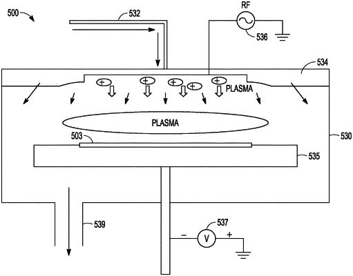
dielectric films in the memory array providing electrical isolation, the dielectric films including a spin-on dielectric (SOD) as a dielectric between stacks of memory cells of the memory array, with the SOD including carbon and plasma-implanted ions, the SOD having a carbon content that varies along a length of the SOD.