| CPC G09F 9/301 (2013.01) [H10K 50/84 (2023.02); H10K 59/122 (2023.02); H10K 59/131 (2023.02); H10K 2102/102 (2023.02); H10K 2102/103 (2023.02); H10K 2102/311 (2023.02)] | 20 Claims |
|
1. A display device, comprising:
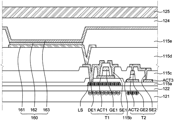
a display panel having a display area and a non-display area, the display panel including a substrate;
a transistor disposed above the substrate in the display area;
a flexible film disposed on a side surface of the non-display area, the flexible film connected to the substrate;
a connection member disposed from an outermost side surface of the display panel to an upper surface of the display panel and electrically connected to the flexible film; and
a conductive layer disposed below the substrate, the conductive layer electrically connected to the connection member,
wherein the connection member is structured to distribute a low potential power voltage from the flexible film to the conductive layer to offset positive charges trapped below the transistor.
|