| CPC G02B 6/124 (2013.01) [G01S 7/4817 (2013.01)] | 8 Claims |
|
1. An optical device comprising:
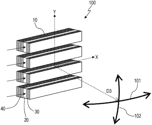
a first mirror having a first reflecting surface and extending along a first direction;
a second mirror having a second reflecting surface that faces the first reflecting surface and extending along the first direction;
an optical waveguide layer, located between the first mirror and the second mirror, that causes light to propagate along the first direction, wherein:
a transmittance of the first mirror is higher than a transmittance of the second mirror,
a reflection spectrum of at least either the first mirror or the second mirror with respect to light arriving from a direction normal to the reflecting surface includes, in a wavelength region in which a reflectance is higher than or equal to 90%, a local maximum point and first and second points of inflection located closer to a long-wavelength side than the local maximum point, and
a reflectance monotonically decreases on a long-wavelength side of the local maximum point to at least the second point of inflection.
|